Delivering smarter, more efficient defect classification for advanced manufacturing
Mon, 03/13/2023 - 12:00
This Singapore Deep Tech startup is using artificial intelligence to bring more efficiency to high-volume and high-complexity manufacturing, starting with the semiconductor industry.
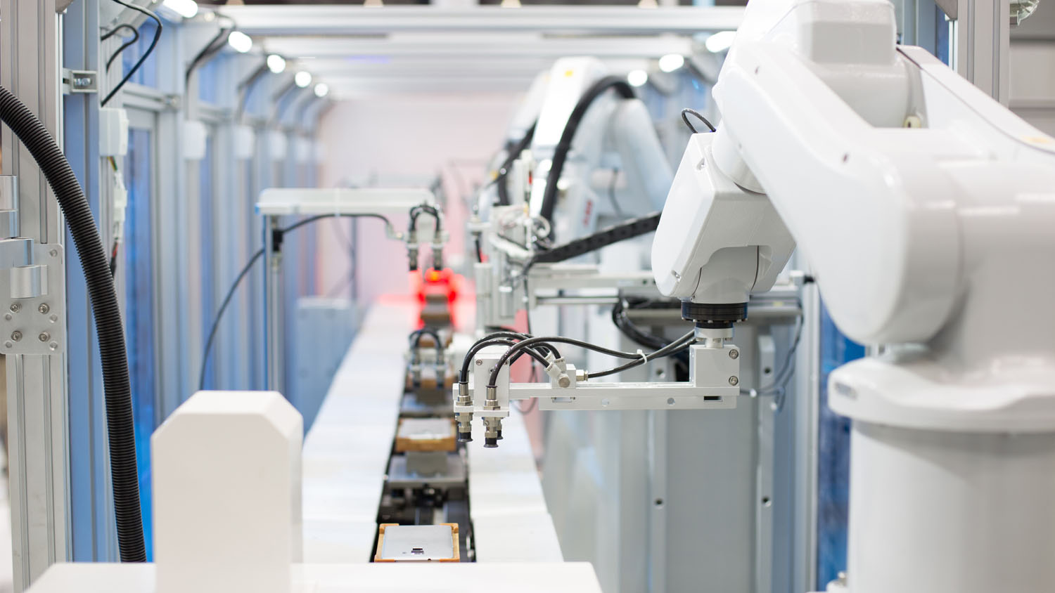
The first time SixSense co-founder and Chief Technology Officer Avni Agrawal stepped inside a semiconductor manufacturing plant, she was surprised to see human workers among the robotic arms, manually reviewing and classifying images into different defect categories.
“Even though the semiconductor industry is highly automated, the visual inspection process remains fairly manual,” says Agrawal. “This leads to a lot of downstream problems in manufacturing which are very significant for them.”
Image of a worker inspecting a semiconductor microchip.
Coupled with the exponential growth of high-powered devices dependent on semiconductors, Agrawal and her co-founder, Akanksha Jagwani, saw this bottleneck as an opportunity to help reduce costs and revenue losses while increasing productivity in the industry.
The Singapore-based Deep Tech startup has developed an artificial intelligence (AI) powered visual inspection platform designed to make semiconductor manufacturers’ quality inspection processes smarter, more consistent, and more efficient.
“Demand for semiconductors is increasing exponentially, which is going to drive huge growth across the industry,” says Agrawal. “Manufacturers are looking to increase automation in areas that will help them to scale.”
An intelligent approach to identifying and pre-empting defects
SixSense’s software platform enables semiconductor manufacturers to review millions of images of products at high speed, identifying and classifying defects automatically using deep learning and computer vision.
Compared to other defect identification solutions, SixSense offers higher accuracy for a broad range of defects as it mimics human behaviour during classification. For example, by looking at several images taken from a variety of angles to classify some types of defects, rather than just one.
Once a defect is detected, it is then sent for manual classification and retraining, ensuring engineers are fully aware of when and where defects are occurring. The system also provides engineers with an explanation of every decision it makes, providing unparalleled transparency.
The platform – which can be configured in just a few hours for any kind of image data and defect type – also alerts engineers when a new defect type happens across the company’s processes.
Using the SixSense platform helps manufacturers to significantly reduce the time and cost of inspecting products, and avoid reputational damage and costs associated with failures.
A meeting of entrepreneurial minds
The SixSense story began in 2018 when computer scientist Agrawal met mechanical engineer Jagwani through the Entrepreneur First programme.
Avni Agrawal (right) and Akanksha Jagwani (left) at a semiconductor conference held at Singapore’s Marina Bay Sands.
Discovering a shared interest in using AI and machine learning in manufacturing, the pair co-founded SixSense, of which Jagwani is now Chief Executive Officer. After consulting more than 50 engineers – many of whom were from the semiconductor industry – the pair decided to focus on creating a better way to manage defect inspections in the semiconductor industry.
“Having worked at Visa, I had worked with huge volumes of data previously and seen how the financial services industry had developed a lot of innovative solutions around that,” Agrawal says. “I was interested in building something in the AI and machine learning space for a more orthodox industry.”
More than four years on, SixSense software platform is used by some of the world’s leading semiconductor manufacturers based in Asia, Europe and the United States. These manufacturers supply the likes of Rolex, Apple, Microsoft, Google and Samsung.
“In the last few years, since COVID hit, we’ve found that manufacturers have become even more focused on automation because they now understand that relying on manual processes can affect business in ways they didn’t anticipate before,” adds Agrawal.
SixSense has also secured funding from a variety of investors, including SGInnovate and Tin Men Capital. This support is helping the startup to increase the adoption of its product in different geographic markets and test it in other high-tech manufacturing verticals.
Planning for a high-growth future
While it is still early days for the company, Agrawal believes in its enormous potential.
According to Fortune Business Insights, the global semiconductor market was worth US$528 billion in 2021. This is projected to grow to US$1,381 billion by 2029.
“We estimate that our size could be between US$2 billion and US$8 billion in the semiconductor industry alone,” says Agrawal. “But since our technology isn’t limited to semiconductors, our growth could be much faster.”
By improving the chip yield of electronics including electric vehicles, SixSense is also helping to speed up the world’s transition to electrification and net zero emissions.
“We are looking at other high-volume, high-complexity manufacturing verticals because those are the areas where, if a defect occurs, it matters to them. So, areas like advanced manufacturing, electronics, automotive and heavy machinery manufacturing.”
Read our report on trends shaping advanced manufacturing in Asia Pacific.
In the short- to medium-term, the company plans to refine and scale its technology further. It will also invest in building a business development and sales team to help drive growth, and in scaling its customer support in all its geographic markets. Agrawal and Jagwani also want to ensure the company achieves profitability as soon as possible.
In the meantime, the pair is grateful for the support Singapore’s Deep Tech ecosystem has provided so far.
The SixSense team.
“Both Entrepreneur First and SGInnovate are very supportive of companies that are making a dent in this space,” Agrawal says. “And the good thing is that they understand Deep Tech companies can’t get started on day one. It takes time to research the technology. It takes time to build it. It takes time for companies to adopt it.
“We received the space we needed to research the problem, then build a good solution for it.”
On a personal level, she says it has been ‘magical’ to see the dream she and Jagwani first envisioned in 2018 turning into reality.
“It is very inspiring to tackle a problem that is so huge, and then actually solve it.”
Discover more about the innovative startups that SGInnovate supports.
Trending Posts
- A Guide to Singapore’s Hydrogen Ecosystem
- Walking the tightrope of disclosure to create a robust IP strategy
- Why intellectual property (IP) strategy can mean the difference between life and death for a startup
- Going behind-the-scenes in a MedTech startup for a 6-month internship to create lasting impact
- A Guide to Singapore’s Quantum Ecosystem


